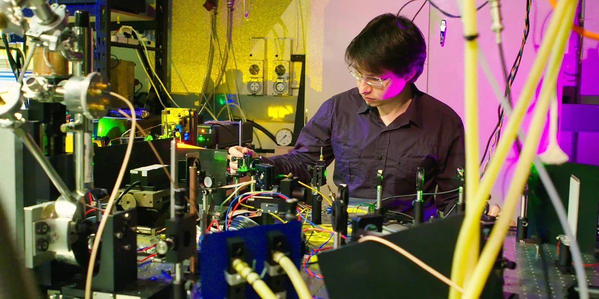
Clean Energy
In this project, we will characterise actual device solar cell structures with electron microscopy techniques and seek to understand the microscopic effects behind the device performance and reliability
A/Prof Jennifer Wong-Leung

This project aims to develop new plasma processing techniques which can be used to generate complex nanostructured surface morphologies on a range of mateirals. These materials have potential applications in a wide range of areas, including catalysis, high energy-density batteries, and anti-reflection coatings.
Dr Matt Thompson, A/Prof Cormac Corr

This is an all-encompassing program to integrate highly sophisticated theoretical modelling, material growth and nanofabrication capabilities to develop high performance semiconductor nanowire array solar cells. It will lead to understanding of the underlying photovoltaic mechanisms in nanowires and design of novel solar cell architectures.
Professor Lan Fu, Dr Ziyuan Li, Professor Chennupati Jagadish AC
Materials Science and Engineering
In this project, we will characterise actual device solar cell structures with electron microscopy techniques and seek to understand the microscopic effects behind the device performance and reliability
A/Prof Jennifer Wong-Leung

The equilibrium shape of voids or crystals is largely influenced by the total surface energies encompassing these 3D objects. This aim of this project is to extract the surface energies of different planes from transmission electron microscopy images of faceted voids and nanowires.
A/Prof Jennifer Wong-Leung

This project aims to investigate the growth of III-V semiconductors on pre-patterned nanotemplates. By using different shapes and geometries, it is envisaged that these nanostructures will provide novel architectures for advanced, next generation optoelectronic devices.
Professor Hoe Tan, Professor Chennupati Jagadish AC
This projects combines ion implantation and deep level transient spectroscopy to study electrically active deep level defects in wide bandgap semiconductors.
A/Prof Jennifer Wong-Leung

This project investigates the structure and density of defects created in 2D materials by energetic ion irradiation, and studies how such defects affect the physical properties of this important class of materials.
Professor Robert Elliman

Contact resistance is becoming a major limitation to device performance and new strategies are required to meet the needs of next-generation devices. Existing contacts typically exploit the thermal and chemical stability of silicide/Si interfaces and take the form of a metal/silicide/Si heterostructure (e.g. W/TiN/TiSi2/Si), with the contact resistance dominated by the silicide/Si interface. The contact resistance of this interface is limited by the doping concentration in the Si substrate and the Schottky barrier height (SBH) of the heterojunction. However, doping concentrations already exceed equilibrium solid solubility limits and further increases achieve only minor improvements. Instead, any further reduction in contact resistivity relies on reducing the SBH. This project will explore methods for controlling the SBH and develop device structures for measuring ultra-low contact resistivities.
Professor Robert Elliman, Mr Tom Ratcliff

Uniform composition and tunability over the emission wavelength of ternary nanowires is an important challenge for nanowire growth. Growth of nanowires combined with a range of characterisation techniques including electron microscopy will be used for this project. PhD studentships currently available.
A/Prof Jennifer Wong-Leung, Professor Hoe Tan

Study the formation and stability of high energy ion tracks in minerals under controlled environments with importance for geological dating techniques.
Prof Patrick Kluth

The hexagonal form of sp3 bonded carbon is predicted to be harder than 'normal' cubic diamond. We can make tiny amounts of this new form of diamond and want to know if it really is harder than diamond.
Prof Jodie Bradby

Scanning electron microscopy is a powerful tool for materials and this method is believed to correctly identify depletion regions in semiconductor devices. This project links the electron microscopy contrast to the depletion regions measured by capacitance-voltage measurements in some devices with an aim to understanding the source of contrast.
A/Prof Jennifer Wong-Leung, Dr Mark Lockrey
The project aims at establishing the possibilities of high-energy electron scattering in the analysis of thin layers.
A/Prof Maarten Vos

We have shown that this fascinating material has different properties depending on the thermal pathways. The effect on how this influences the new phased formed under pressure has not been investigated.
Prof Jodie Bradby
Nuclear fusion is a promising technology for solving the world’s energy crisis while drastically reducing pollution and avoiding the creation of nuclear waste, a major issue for nuclear fission. However, there are many scientific and technical challenges to be overcome before this technology can be used for large-scale energy generation. One of the problems that need to be solved is the tolerance of the diverter walls to the high temperatures and He implantation – conditions that are prevalent inside the fusion reactors.
A/Prof Cormac Corr

New forms of materials can be made using extreme pressures via diamond anvil cells.
Prof Jodie Bradby

Interest in biomimetic computing has led to interest in an excting new range of of solid-state neurons and synapses based on non-volatile resistive-switching and volatile threshold-switching in metal-oxide thin films. This project will explore the operation and functionality of these new devices.
Professor Robert Elliman, Dr Sanjoy Nandi

Investigate the fascinating porous structures of ion irradiated antimony based semiconductors and utlise them to built proptotype sensing devices or thermolectric generators.
Prof Patrick Kluth, Dr Christian Notthoff

This project will combine experimental work, computer simulation and modelling to investigate the physical processes underpinning resistive switching in transition metal oxides (e.g. Ta2O5, HfO2, Nb2O5 and NbO2) and to explore its application in future non-volatile memory (i.e. ReRAM) devices.
Professor Robert Elliman, Dr Sanjoy Nandi

This project involves studying the complex plasma-surface interaction region of a fusion-relevant plasma environment through laser-based and spectroscopic techniques.
A/Prof Cormac Corr, Dr Matt Thompson

Fusion energy promises millions of years of clean energy, but puts extreme stress on materials. This research will resolve scientific issues surrounding plasma-material interactions to guide and facilitate development of future advanced materials for fusion reactors.
A/Prof Cormac Corr, Prof Patrick Kluth, Dr Matt Thompson
Nanoscience and Nanotechnology

The equilibrium shape of voids or crystals is largely influenced by the total surface energies encompassing these 3D objects. This aim of this project is to extract the surface energies of different planes from transmission electron microscopy images of faceted voids and nanowires.
A/Prof Jennifer Wong-Leung

This project aims to investigate the growth of III-V semiconductors on pre-patterned nanotemplates. By using different shapes and geometries, it is envisaged that these nanostructures will provide novel architectures for advanced, next generation optoelectronic devices.
Professor Hoe Tan, Professor Chennupati Jagadish AC

Experimental and theoretical work on the development of novel nanostructured materials with unusual optical properties. Special attention to our research is the development of tunable and functional nanostructured metamaterials that interact strongly with light. Such materials underpin novel optical technologies ranging from wearable sensors to night-vision devices.
Prof Dragomir Neshev, Dr Andrei Komar, Dr Mohsen Rahmani

The project aims to investigate compound semiconductor micro-ring lasers on silicon substrates using selective area growth to engineer the shape of the lasing cavity at the nano/micro-scale. This project will open up new doors to the industry since an integrated laser which is reliable, efficient and easily manufacturable is still elusive in Si photonics.
Professor Hoe Tan, Professor Chennupati Jagadish AC

This project investigates the structure and density of defects created in 2D materials by energetic ion irradiation, and studies how such defects affect the physical properties of this important class of materials.
Professor Robert Elliman

Contact resistance is becoming a major limitation to device performance and new strategies are required to meet the needs of next-generation devices. Existing contacts typically exploit the thermal and chemical stability of silicide/Si interfaces and take the form of a metal/silicide/Si heterostructure (e.g. W/TiN/TiSi2/Si), with the contact resistance dominated by the silicide/Si interface. The contact resistance of this interface is limited by the doping concentration in the Si substrate and the Schottky barrier height (SBH) of the heterojunction. However, doping concentrations already exceed equilibrium solid solubility limits and further increases achieve only minor improvements. Instead, any further reduction in contact resistivity relies on reducing the SBH. This project will explore methods for controlling the SBH and develop device structures for measuring ultra-low contact resistivities.
Professor Robert Elliman, Mr Tom Ratcliff

Uniform composition and tunability over the emission wavelength of ternary nanowires is an important challenge for nanowire growth. Growth of nanowires combined with a range of characterisation techniques including electron microscopy will be used for this project. PhD studentships currently available.
A/Prof Jennifer Wong-Leung, Professor Hoe Tan

This project aims to investigate the concepts and strategies required to produce electrically injected semiconductor nanowire lasers by understanding light interaction in nanowires, designing appropriate structures to inject current, engineer the optical profile and developing nano-fabrication technologies. Electrically operated nanowire lasers would enable practical applications in nanophotonics.
Professor Chennupati Jagadish AC, Professor Hoe Tan

Study the formation and stability of high energy ion tracks in minerals under controlled environments with importance for geological dating techniques.
Prof Patrick Kluth

Scanning electron microscopy is a powerful tool for materials and this method is believed to correctly identify depletion regions in semiconductor devices. This project links the electron microscopy contrast to the depletion regions measured by capacitance-voltage measurements in some devices with an aim to understanding the source of contrast.
A/Prof Jennifer Wong-Leung, Dr Mark Lockrey

Semiconductor nanowires are emerging nano-materials with substantial opportunities for novel photonic and electronic device applications. This project aims at developing a new generation of high performance NW based photodetectors for a wide range of applications.
Professor Lan Fu, Dr Ziyuan Li, Professor Hoe Tan

Interest in biomimetic computing has led to interest in an excting new range of of solid-state neurons and synapses based on non-volatile resistive-switching and volatile threshold-switching in metal-oxide thin films. This project will explore the operation and functionality of these new devices.
Professor Robert Elliman, Dr Sanjoy Nandi

Investigate the fascinating porous structures of ion irradiated antimony based semiconductors and utlise them to built proptotype sensing devices or thermolectric generators.
Prof Patrick Kluth, Dr Christian Notthoff

This project will combine experimental work, computer simulation and modelling to investigate the physical processes underpinning resistive switching in transition metal oxides (e.g. Ta2O5, HfO2, Nb2O5 and NbO2) and to explore its application in future non-volatile memory (i.e. ReRAM) devices.
Professor Robert Elliman, Dr Sanjoy Nandi

Auger electrons are emitted after nuclear decay and are used for medical purposes. The number of Auger electrons generated per nuclear decay is not known accurately, a fact that hinders medical applications. This project aims to obtain a experimental estimate of the number of Auger electrons emitted per nuclear decay.
A/Prof Maarten Vos, Dr Tibor Kibedi, Professor Andrew Stuchbery

This is an all-encompassing program to integrate highly sophisticated theoretical modelling, material growth and nanofabrication capabilities to develop high performance semiconductor nanowire array solar cells. It will lead to understanding of the underlying photovoltaic mechanisms in nanowires and design of novel solar cell architectures.
Professor Lan Fu, Dr Ziyuan Li, Professor Chennupati Jagadish AC
Photonics, Lasers and Nonlinear Optics

Experimental and theoretical work on the development of novel nanostructured materials with unusual optical properties. Special attention to our research is the development of tunable and functional nanostructured metamaterials that interact strongly with light. Such materials underpin novel optical technologies ranging from wearable sensors to night-vision devices.
Prof Dragomir Neshev, Dr Andrei Komar, Dr Mohsen Rahmani

The project aims to investigate compound semiconductor micro-ring lasers on silicon substrates using selective area growth to engineer the shape of the lasing cavity at the nano/micro-scale. This project will open up new doors to the industry since an integrated laser which is reliable, efficient and easily manufacturable is still elusive in Si photonics.
Professor Hoe Tan, Professor Chennupati Jagadish AC

This project aims to investigate the concepts and strategies required to produce electrically injected semiconductor nanowire lasers by understanding light interaction in nanowires, designing appropriate structures to inject current, engineer the optical profile and developing nano-fabrication technologies. Electrically operated nanowire lasers would enable practical applications in nanophotonics.
Professor Chennupati Jagadish AC, Professor Hoe Tan

Antennas are at the heart of modern radio and microwave frequency communications technologies. They are the front-ends in satellites, cell-phones, laptops and other devices that make communication by sending and receiving radio waves. This project aims to design analog of optical nanoantennas for visible light for advanced optical communiction.
Prof Dragomir Neshev, Dr Andrey Miroshnichenko

Semiconductor nanowires are emerging nano-materials with substantial opportunities for novel photonic and electronic device applications. This project aims at developing a new generation of high performance NW based photodetectors for a wide range of applications.
Professor Lan Fu, Dr Ziyuan Li, Professor Hoe Tan
Plasma Applications and Technology

This project aims to develop new plasma processing techniques which can be used to generate complex nanostructured surface morphologies on a range of mateirals. These materials have potential applications in a wide range of areas, including catalysis, high energy-density batteries, and anti-reflection coatings.
Dr Matt Thompson, A/Prof Cormac Corr

Plasma agriculture is an innovative field that applies plasma to agriculture processes such as farming, food production, food processing, and food preservation. In agriculture, plasmas may be used to eradicate all microorganisms; bacterial, fungal and viral particles in fruit and vegetables.
A/Prof Cormac Corr

Plasma–liquid interactions are an important topic in the field of plasma science and technology. The interaction of non-equilibrium plasmas with a liquid have many important applications ranging from environmental remediation to material science and health care.
A/Prof Cormac Corr