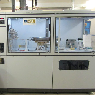
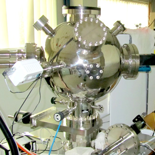
The group conducts state-of-the-art research in the epitaxial growth of novel semiconductor nanostructures using 3 metal-organic chemical vapour deposition systems, such as nanowires, nano-membranes, micro-rings, quantum wells and quantum dots. Understanding the fundamental growth mechanisms through extensive materials characterisation is important to be able to control the growth of these nanostructures.
These nanostructures are then incorporated into various optoelectronic devices such as lasers, LEDs, photodetectors, solar cells and bio/chemical sensors. The use of the nanostructures in these devices are expected to result in properties and performance not achievable in those made of their bulk counterparts, leading to new applications. For example, nanowires with their large surface-area-to-volume ratio are advantageous for solar cell, photodetector and sensor applications. Micro-rings formed through bottom up growth have excellent facets resulting in very high quality-factor cavities. Our ability to grow semiconductor nanostructures of different shapes opens up the prospect of making active metasurfaces to compensate for optical losses. Our semiconductor nanostructures will be incorporated into miniaturised meta-optical systems and used to tailor the various properties of light, such as intensity, phase, polarisation and spatial mode, with unprecedented accuracy for applications in holographic displays, LiDAR systems, Li-Fi, augmented reality, optical and quantum communications, remote sensing and wearable sensors.
The group’s research also spans broadly on materials, electrochemical devices and system integration for green hydrogen generation. More specifically, our expertise comprises engineering of advanced catalytic and semiconductor materials, photoelectrochemical cells for direct solar-to-hydrogen production, design of low-cost electrodes stacks, and development of next generation electrochemical technologies.
We utilised the state-of-the-art cleanroom fabrication facility of ANFF, ACT Node to synthesise our materials and fabricate our devices. Some of these facilities include advanced high throughput, high resolution electron beam lithography system, nanoimprint and photolithography, plasma etching and deposition systems, atomic layer deposition system and focussed ion beam system.
III-V compound semiconductors are a different class of semiconductors that have unique properties not found in the more well known silicon. Our research deals from the growth of these materials to the structural, electrical and optical characterisation in order to understand the growth mechanism and material properties.
Wide bandgap semiconductors are typically characterised by their bandgap which is several of eVs. Examples of semiconductors that fall into this category are SiC, GaN, ZnO and their related compounds.
Quantum confined structures are utilised in a variety of applications due to the quantum confinement effect which forms the basis for improved device characteristics. The mature epitaxy technology has allowed us to grow quantum well and dot structures with unique electronic and optical properties.
Nanowire research is a new and emerging field growing at a fast pace. The excitement in this field is due to the unique electronic and optical properties of the nanowires. The unique properties stem from their large surface to volume ratio, very high aspect ratio, and carrier and photon confinement in two dimensions.
Semiconductor lasers have very broad applications; they can be mass produced and easily integrated. Semiconductor lasers have found a widespread use as pumps for solid state lasers and are also heavily integrated into long distance fibre optic communication systems.
Photodetectors are typically fabricated from semiconductors and are used to detect/absorb photons, which are then converted to electrical signals.
Semiconductor nanowires hold outstanding potential as key components of future devices and systems. Offering reduced dimensionality, outstanding materials properties and the capability for bottom-up assembly, these nanostructures are highly promising nanobuilding blocks.
With a reduction in size, unique electrical, mechanical, chemical and optical properties have been reported in semiconductor nanowires, offering an unprecedented broad range of applications. These applications encompass various disciplines of science and engineering such as electronics, photonics, biomedical sensors and communications.
The average solar cell that you might see on the roof of a house has an efficiency of about 10 to 15% and usually made of silicon. One class of semiconductor frequently used in efficient solar cells is the III-Vs, where efficiencies of over 40% are possible when the cells are coupled with external optical concentrators.
Bringing down the cost of electricity generated from solar radiation using photovoltaics has been the focus of intense investigations in recent years. By employing light trapping techniques to increase the path-length of light, the total absorption inside a thin absorber layer can be enhanced.
Hydrogen has long been described as the fuel of the future, as it can be produced abundantly and is clean-burning. With recent multi-billion dollar investment in large-scale production of green hydrogen in Australia and around the globe, there is not a better time to engage in this field.

