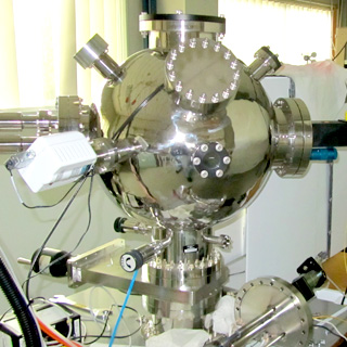
Pulsed laser deposition system
This class of semiconductors is typically characterised by their bandgap which is several of eVs. Examples of semiconductors that fall into this category are SiC, GaN, ZnO and their related compounds. The large bandgap nature of these materials is often exploited for applications in visible-UV optoelectronic devices (such as UV/blue/green LEDs/laser diodes, solar-blind detectors), high temperature and high power electronic components.
The realisation of devices for these wide bandgap semiconductors hinges on the understanding and characterisation of these semiconductors as grown and after different semiconductor processing, for instance doping, ion implantation, contact formation. In addition pulsed laser deposition of non-polar and polar ZnO epilayers and their heterostructures for polarization engineering and transport/scattering mechanisms studies is also investigated. This will lead to the development of advanced high electron mobility transistors and photodetectors.
The department is expecting the delivery of a new MOCVD reactor in late-2012 for the deposition of GaN and related materials.
