
| Position | Research Fellow |
|---|---|
| Department | Electronic Materials Engineering |
| Research group | Semiconductor optoelectronics and nanotechnology group |
| Office | Physics New 3 13 |
| Webpage | https://www.linkedin.com/in/wei-wen... |
Bottom-up fabrication of laser cavities via epitaxial growth is a compelling alternative to conventional top-down methods, offering micro- and nanolasers with ultra-low optical losses. By avoiding etching-induced roughness, this approach produces atomically smooth crystal facets and high-quality optical confinement at the nanoscale.
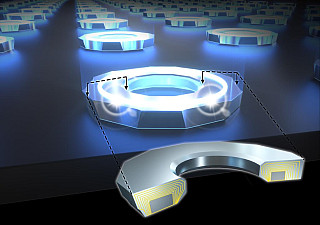
This project aims to demonstrate electrically injected lasing in InP/InAsP multi-quantum well micro-ring cavities, realized through selective area epitaxy. The platform combines the precision of epitaxial growth with the scalability of on-chip integration, addressing a key challenge in advancing bottom-up nanolasers to practical device architectures.
The resulting microcavity lasers promise wide-ranging applications in telecommunications, precision sensing, and as compact light sources for next-generation photonic integrated circuits. By enabling electrically driven operation in epitaxially grown nanocavities, this work will lay the foundation for robust, scalable, and energy-efficient nanoscale light sources that can transform integrated nanophotonics.

Monolithic integration of III-V semiconductor lasers on silicon platforms has long been viewed as the “holy grail” of Si photonics, as it would resolve the long-standing challenge of integrating efficient light sources directly onto silicon chips. Si photonics underpins the data interconnects that enable cloud computing and artificial intelligence data centres, where energy efficiency and bandwidth are critical. However, the absence of a native on-chip laser remains a major bottleneck to fully unlocking the potential of this technology.
While planar growth of III-V materials on Si has been widely demonstrated, direct epitaxy of III-V nanostructures on Si remains highly challenging due to the large lattice mismatch, which introduces defects, and the surface polarity mismatch, which leads to anti-phase boundaries. This project seeks to address these barriers by engineering the III-V/Si interfacial energy to enable the direct growth of InP/InAsP light-emitting nanostructures on Si. Success would pave the way for efficient, scalable integration of active photonic components, accelerating advances in next-generation AI-driven data infrastructure.
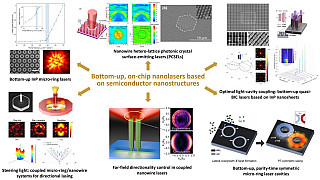
On-chip coherent light sources are a cornerstone of integrated photonics, yet current nanolasers face fundamental limitations due to fabrication-induced scattering losses. This project pursues a bottom-up epitaxial approach to nanolaser cavities, where atomically smooth crystal facets naturally formed during growth eliminate the defects inherent to top-down fabrication. These high-quality, sub-wavelength dielectric cavities confine light with exceptional efficiency, enabling stronger light–matter interaction and reduced lasing thresholds.
Building on recent demonstrations of bottom-up micro-rings, nanowires, photonic crystal surface-emitting lasers (PCSELs), and quasi-bound state in the continuum (BIC) metasurfaces, the research will push towards next-generation designs, including flatband and topological nanolasers. By leveraging unique photonic band structures, these novel cavities promise robust, scalable, and disorder-immune operation. Ultimately, the project seeks to redefine nanoscale laser technology, opening new pathways for compact, high-performance photonic integration.
The efficiency of light-emitting diodes (LEDs) in the green–yellow spectral range remains limited by the well-known “green gap,” where device performance drops sharply compared to blue and red emitters. Closing this gap is essential not only for high-efficiency solid-state lighting but also for achieving high color rendering and “true” white displays based on the full RGB spectrum—capabilities critical for next-generation lighting, microdisplays, and imaging technologies.
This project explores a new route to green emission by engineering the crystal phase of GaP and AlInP nanostructures. By transforming these materials from their conventional cubic zinc blende structure to the hexagonal wurtzite phase, they can be converted from indirect to direct bandgap semiconductors, enabling strong radiative recombination in the green region.
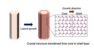
A promising pathway is the crystal structure transfer method, where nanostructures grown along specific crystallographic directions preserve the wurtzite phase of a core template. This strategy effectively “transfers” the crystal phase, offering a scalable route to efficient green LEDs.