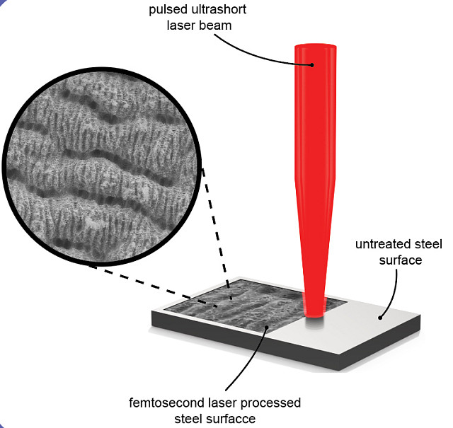
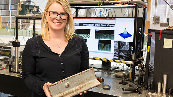
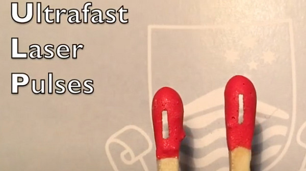
Laser processing is a cutting-edge technique designed for to clean, texture, enhance surfaces in a way not possible with any other method. It is a non-contact process, which does not require the use of chemicals or abrasives, thus eliminating problems of chemical toxicity, corrosive residues, erosion and blurring of surface detail.
Laser processing is being rapidly adopted as an industrial process from cleaning large civil engineering infrastructure through to high-precision micro structuring. The recent emergence of a new generation of ultrashort-pulse lasers with average powers exceeding 100 W offers high throughput processing of large surface areas whilst retaining micron-scale precision.
We evaluate the processing rate and efficiency and the cost efficiency of high-power laser in large-scale industrial processes. The analysis accounts for single pulse energy (dependent on repetition-rate), the focussed laser spot size (determined by the focusing optics), the resulting laser fluence, all linked to the material parameters.
As the cost of laser power is continuously driven lower by improved laser designs/technology/manufacturing, ultrashort laser processing is readily approaching 24/7 use in factory conditions, stretching the boundaries of laser surface processing. This motivates research into and optimisation of process parameters to maximise productivity and so speed deployment.

Our research program is divided into three streams:


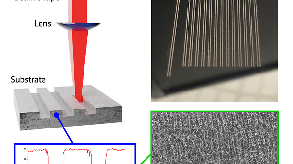
The mainstay here is the Light Conversion Carbide laser, which produces 40W average power in pulses from 275 fs to 18 ps and repetition rates up to 1 MHz. Maximum pulse energy is 400 microJoules at 1026 nm. The unit is also equipped with a fully automated harmonic generator which provides up to 26W of 513 nm visible light and 13W of 342 nm UV light. This is sufficient power to cut/surface structure most materials at reasonable rates with high quality cut faces and potentially no thermal damage. With a high-speed scanning system, we have demonstrated sub 5*C temperature rises in material as thin as 10 microns during ablation at a maximum rate of 7 mm3/min for stainless steel ablated with 1030 nm. We have polygon scanner systems for 1030 nm, and galvanometer/mechanical stage systems for all wavelengths. With beam homogenization, edge profiles can be very nice as shown below. For the Polygon system the maximum scan field is 280 x 280 mm, and the minimum spot size is about 30 microns.
Please contact us to discuss more if you are interested.