Monolithic integration of III-V semiconductor lasers on silicon platforms has long been viewed as the “holy grail” of Si photonics, as it would resolve the long-standing challenge of integrating efficient light sources directly onto silicon chips. Si photonics underpins the data interconnects that enable cloud computing and artificial intelligence data centres, where energy efficiency and bandwidth are critical. However, the absence of a native on-chip laser remains a major bottleneck to fully unlocking the potential of this technology.
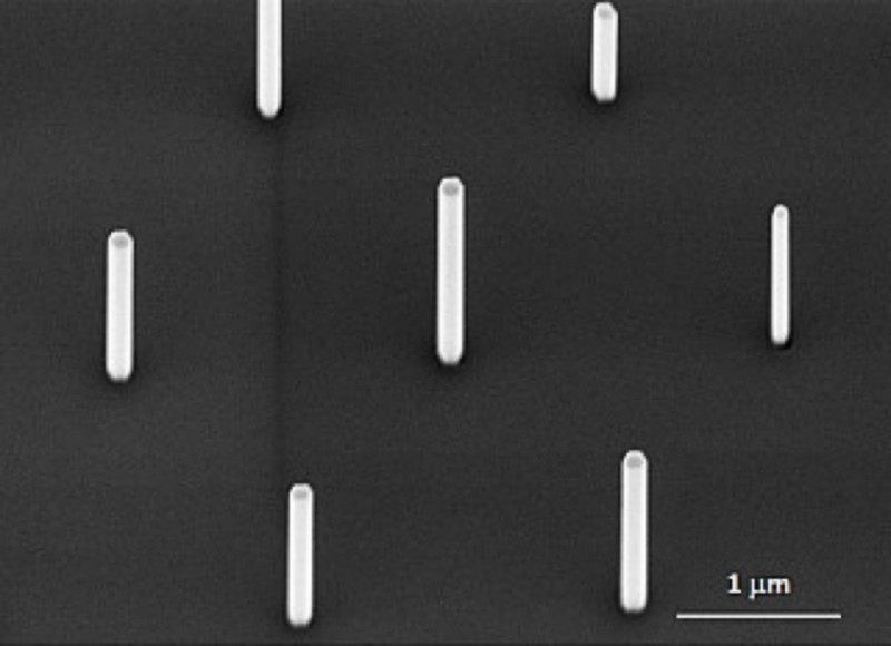
While planar growth of III-V materials on Si has been widely demonstrated, direct epitaxy of III-V nanostructures on Si remains highly challenging due to the large lattice mismatch, which introduces defects, and the surface polarity mismatch, which leads to anti-phase boundaries. This project seeks to address these barriers by engineering the III-V/Si interfacial energy to enable the direct growth of InP/InAsP light-emitting nanostructures on Si. Success would pave the way for efficient, scalable integration of active photonic components, accelerating advances in next-generation AI-driven data infrastructure.


