The nitrogen-vacancy (NV) centre in diamond is a premier solid-state defect for quantum information processing and metrology. An integrated diamond quantum device harnesses the collective properties of multiple NV centres, enabling room-temperature quantum computing, sensing, and demonstrations of fundamental physics. While large-scale devices are poised to fill an important gap in the burgeoning quantum technology landscape, their practical realisation is not possible using current top-down fabrication techniques such as ion implantation. For example, the ultimate capabilities of quantum sensors will require uniformity in NV centre properties, whereas room-temperature quantum computing will require the fabrication of strongly coupled NV centres at scale. Consequently, this necessitates the development of a bottom-up fabrication technique which is scalable, deterministic, and possesses atomic-scale precision.
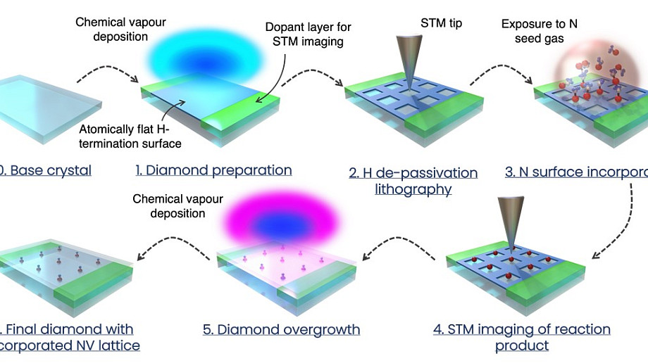
Informed by existing methods for fabricating phosphorous defects in silicon, I envision a scanning-probe lithography technique for atomically precise manufacturing of NV centres in diamond. Hence, in this talk I outline a viable multi-step procedure for scalable fabrication of diamond quantum devices. This entails creation of active surface sites through hydrogen desorption lithography, chemical adsorption of a N-containing molecule, and diamond overgrowth to form a bulk NV centre. A combination of theory, electrostatic modelling, and first-principles calculations are used to systematically validate the feasibility of each step. While there exist significant engineering and technical challenges facing bottom-up NV fabrication, I conclude that these are surmountable, and there are no fundamental barriers to constructing a scalable room-temperature device.
Join the Zoom Meeting
Meeting ID: 867 4902 2737
Password: 261725
https://anu.zoom.us/j/86749022737?pwd=WXJ2dk5FTTNjRzJvdTgvVVhIZW9HZz09
Room:
Conference Room (4.03)