Hexagonal boron nitride (hBN) is a two-dimensional (2D) material that has attracted considerable attention in recent years. As a wide bandgap semiconductor with excellent thermal/chemical stability, it has been widely utilized as a gate dielectric in field effect devices or surface passivation of other materials 2D materials. hBN is also a highly luminescent material and its optical properties have been the subject of numerous studies in the past. Emissions from hBN range from near band-edge (215 nm) to sub-bandgap luminescence that extend from UV (300-330 nm) to visible wavelengths (570 – 750 nm). In spite of having an indirect bandgap (of 5.955 eV [1]), its ability to emit light, with luminescent efficiencies (~ IQE of 50 %) comparable to direct bandgap materials makes it an unusual and unique material [2, 3].
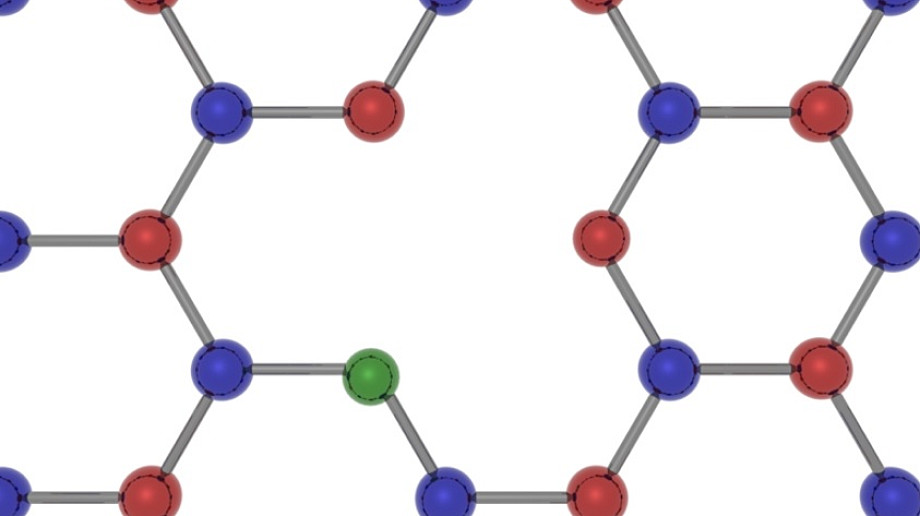
Recently, single photon emission (SPE) from defects in hBN have generated new interests in this material as a source of bright, stable and robust quantum emitters [4]. However, despite the vast range of experimental results and theoretical calculations, the defect structure responsible for single photon emission from hBN has remained elusive. Epitaxially grown hBN, using techniques like metal organic vapour phase epitaxy (MOVPE), molecular beam epitaxy (MBE) and chemical vapor deposition (CVD) has provided valuable insight in to the origins of sub-bandgap luminescence from hBN. By controlling the incorporation of impurities into hBN and comparing various synthesis methods (MOVPE, CVD and MBE), direct evidence that the visible SPEs are carbon related has been obtained. Room temperature optically detected magnetic resonance is demonstrated on ensembles of these defects. Furthermore, ion implantation experiments were performed on MOVPE grown hBN. Results confirm that only ‘carbon’ implantation in hBN created SPEs in the visible spectral range. Computational analysis of hundreds of potential carbon-based defect transitions suggest that the emission results from the negatively charged VBCN− defect, which experiences long-range out-of-plane deformations and is environmentally sensitive. Our results resolve a long-standing debate about the origin of single emitters at the visible range in hBN and will be key to deterministic engineering of these defects for quantum photonic devices.
1. Cassabois, G., P. Valvin, and B. Gil, Hexagonal boron nitride is an indirect bandgap semiconductor. Nature Photonics, 2016. 10(4): p. 262.
2. Schué, L., et al., Bright Luminescence from Indirect and Strongly Bound Excitons in h-BN. Physical Review Letters, 2019. 122(6): p. 067401.
3. Léonard, S., et al., Characterization methods dedicated to nanometer-thick hBN layers. 2D Materials, 2017. 4(1): p. 015028.
4. Tran, T.T., et al., Robust Multicolor Single Photon Emission from Point Defects in Hexagonal Boron Nitride. ACS Nano, 2016. 10(8): p. 7331-7338.
Zoom Event https://anu.zoom.us/j/94111701666