
| Position | Postdoctoral Fellow |
|---|---|
| Department | Electronic Materials Engineering |
| Research group | Semiconductor optoelectronics and nanotechnology group |
| Office | Physics New 3 13 |
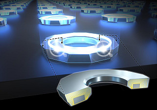
Bottom-up fabrication of lasers via epitaxial growth has been emerging as a promising alternative to the conventional top-down fabrication methods, due to its potential to realise micro-lasers with ultra-low losses. In this project, we aim to demonstrate electrically-injected lasing in InP/InAsP multi-quantum well micro-ring cavities that are grown by the selective area epitaxy technique. These on-chip micro-cavity lasers have a wide range of potential applications, ranging from telecommunication and sensing devices to light sources in next-generation photonic integrated circuits.

Using the selective area epitaxy technique, III-V semiconductors can be grown in the form of pseudo-two dimensional (2D) nanosheet structures. The unique morphology of the nanosheets results in light absorption efficiency which is highly sensitive to the light polarisation. In this project, we aim to demonstrate polarisation-sensitive photodetector devices based on III-V nanosheet arrays, which can potentially be used for optical computing and advanced imaging applications.

Monolithic integration of III-V semiconductor lasers on Si platforms has been the "holy grail" in Si photonics, as it could potentially solve the long-standing light source problem in the technology. While there have been numerous demonstrations of planar growth of III-V materials on Si substrates, growing III-V nanostructures directly on Si is not a trivial task. In this project, we aim to demonstrate the direct growth of InP/InAsP light-emitting nanostructures on Si substrates by engineering the III-V/Si interfacial energy.

Parity-time (PT) symmetry is an intriguing phenomenon in quantum mechanics, whereby a non-Hermitian Hamiltonian that obeys PT symmetry can exhibit completely real eigenvalues. In recent years, the extension of PT symmetry into the field of photonics has led to a plethora of new class of photonics devices that operate based on PT-symmetric exceptional points (EPs), such as PT-symmetric lasers, EP-enhanced sensors, and coherent perfect absorbing (CPA) anti-lasers.
Among these novel devices, PT-symmetric lasers are especially attractive from the perspective of practical applications, as the optical coupling in the system can be engineered to achieve enhanced side mode suppression without compromising the lasing threshold and the fabrication complexity. However, single-mode lasing in PT-symmetric micro-cavity lasers has so far only been demonstrated in systems fabricated by conventional top-down approaches. Meanwhile, bottom-up growth of III-V laser cavities has recently emerged as a promising alternative to the conventional top-down fabrication method, as it can potentially realise micro-cavity lasers with superior sidewall qualities, which is crucial to laser performance especially at the submicron dimensions.
In this project, we aim to explore PT-symmetric lasing in III-V semiconductor micro-cavity lasers that are epitaxially grown on their substrates, free from any etching-induced damage. In particular, we aim to demonstrate performance improvements by exploiting some of the unique features of bottom-up grown laser cavities, such as coupling strength tuning by engineering the cavity sidewall facets, and enhanced lasing efficiencies due to the superior sidewall facet quality.